Embedded Hardware Design Studio

Schematic to Silicon.

We engineer electronics that survive contact with the real world — from first schematic to production-ready hardware. 4+ years turning bold ideas into manufacturable products.

REV 2.4 · SCHEMATIC TO PRODUCTION · UPDATED 2026

STUDIO AT A GLANCE Active
4+
Years Experience
6
Sectors Served
10
Layer PCBs Designed
3
Design Platforms
Currently Designing
Automotive ECU IoT Gateway BMS Platform SOM Carrier Board
01

Hardware Design Courses

Learn on the tools we design with.

Five courses on KiCad and Cadence Allegro / OrCAD. Learn the stage of the product flow you need, or work through all of it, from a product requirement to a validated board.

5 courses · from ₹2,499 · KiCad + Cadence

AXIS ORBIT θ 000°
Design tool
C.01

PCB Design

From schematic basics to Gerber files: symbols, footprints, placement, routing and manufacturing output, on the tool you choose.

KiCad

KiCad Edition

₹2,4991 Month · 12 modules
Who it's for
Students, beginners, hobbyists

Understand the complete PCB design flow and create a simple PCB independently.

View Syllabus12 modules
  1. 01

    PCB Design Introduction

    • What is a PCB?
    • PCB design flow
    • Schematic → Layout → Gerber → Fabrication
    • Understanding layers
  2. 02

    Schematic Basics

    • Reading a schematic
    • Creating a project
    • Placing components
    • Wires and connections
    • Power symbols
    • Net labels
  3. 03

    Creating Symbols

    • What is a schematic symbol?
    • Using existing libraries
    • Basic custom symbol creation
  4. 04

    Schematic Design

    • Build a simple circuit
    • Component selection basics
    • Design organization
    • ERC/DRC introduction
  5. 05

    BOM & Netlist

    • What is BOM?
    • MPN vs component value
    • Generating BOM
    • Understanding nets/netlist
  6. 06

    PCB Footprints

    • What is a footprint?
    • Using standard footprints
    • Basic footprint creation
    • Through-hole vs SMD
  7. 07

    PCB Layout Basics

    • Creating PCB
    • Importing schematic
    • Component placement
    • Basic routing
    • Vias
    • Copper zones
  8. 08

    Placement Fundamentals

    • Why placement matters
    • Decoupling capacitor placement
    • Connector placement
    • Signal flow
    • Basic thermal considerations
  9. 09

    PCB Design Rules

    • Track width
    • Clearance
    • Via selection
    • Design-rule checking
    • Understanding common PCB errors
  10. 10

    PCB Review

    • Basic layout QC
    • 3D view
    • Silkscreen check
    • Connectivity check
  11. 11

    Manufacturing Output

    • What are Gerbers?
    • Drill files
    • Gerber generation
    • Basic fabrication requirements
  12. 12

    Mini Project

    • Complete a simple PCB from schematic → layout → Gerber
Enrol on WhatsApp
Cadence Allegro

Cadence Allegro Edition

₹4,9991 Month · 23 modules
Who it's for
Engineering students, working engineers, PCB designers

Understand the professional PCB development workflow from schematic through manufacturing release.

View Syllabus23 modules
  1. 01

    Industry PCB Design Workflow

    • Product requirement → schematic → PCB → review → fabrication → assembly
    • Roles of HW designer, PCB designer, manufacturer
  2. 02

    Schematic Development

    • Symbol creation
    • Library management
    • Schematic organization
    • Hierarchy
    • Design constraints
    • Power/ground strategy
  3. 03

    Schematic QC

    • ERC/DRC
    • Connectivity verification
    • Unconnected pins
    • Net naming
    • Design review
  4. 04

    BOM Development

    • BOM structure
    • Manufacturer Part Number (MPN)
    • Alternate components
    • Datasheet verification
    • Lifecycle/status
    • BOM QC
  5. 05

    Footprint Creation

    • Footprint creation
    • Datasheet interpretation
    • Land pattern
    • Pad dimensions
    • Solder mask
    • Paste mask
    • Courtyard
  6. 06

    3D / STEP Integration

    • Adding STEP models
    • Orientation
    • Height verification
    • Mechanical interference
    • Connector/mechanical checks
  7. 07

    Footprint QC

    • Pin-1 verification
    • Pin numbering
    • Pad dimensions
    • Body outline
    • Courtyard
    • 3D model verification
  8. 08

    Board Creation

    • Board outline
    • Film/artwork
    • Layer setup
    • Stackup
    • Mechanical layers
    • Board parameters
  9. 09

    Mechanical Integration

    • Import DXF
    • Mechanical drawings
    • Mounting holes
    • Keep-outs
    • Connectors
    • Enclosure constraints
  10. 10

    Netlist & Component Placement

    • Footprint assignment
    • Netlist generation
    • Import netlist
    • Component placement
    • Functional grouping
  11. 11

    Professional Placement Strategy

    • Power flow
    • Signal flow
    • Critical components
    • Decoupling
    • Thermal considerations
    • Connector placement
    • Serviceability
  12. 12

    PCB Routing

    • Track width
    • Clearance
    • Vias
    • Routing strategy
    • Power routing
    • Grounding
    • Differential pairs
    • Critical signals
  13. 13

    Layer & Stackup Strategy

    • 2/4/6/8-layer boards
    • Signal/reference plane relationship
    • Ground planes
    • Power planes
    • Stackup considerations
  14. 14

    Design Constraints

    • Physical constraints
    • Electrical constraints
    • Width/clearance rules
    • Via rules
    • Differential pair rules
    • Length matching
  15. 15

    High-Speed PCB Basics

    • Impedance
    • Differential pairs
    • Return path
    • Crosstalk
    • Length matching
    • USB/Ethernet/DDR concepts
  16. 16

    Power & Thermal Layout

    • High-current routing
    • Copper area
    • Thermal vias
    • Power planes
    • Regulator layout
    • Decoupling strategy
  17. 17

    Layout QC

    • DRC
    • Connectivity
    • Clearance
    • Component orientation
    • Silkscreen
    • Assembly concerns
    • Design-rule review
  18. 18

    Manufacturing Considerations

    • Fabrication capabilities
    • Minimum track/space
    • Via types
    • Annular ring
    • Solder mask
    • Surface finish
    • Panelization basics
  19. 19

    CAM Verification

    • Gerber inspection
    • Drill verification
    • Layer verification
    • Apertures
    • Manufacturing output verification
  20. 20

    Fabrication Documentation

    • FAB notes
    • Layer stackup
    • Board dimensions
    • Material
    • Finish
    • NC drill chart
    • Special manufacturing notes
  21. 21

    Final PCB Review

    • Electrical review
    • Mechanical review
    • Manufacturing review
    • Assembly review
    • Design release checklist
  22. 22

    Gerber Generation

    • Gerber generation
    • NC drill files
    • Pick-and-place data
    • BOM release
    • Manufacturing package
  23. 23

    Industry Project

    • Complete PCB from schematic → libraries → placement → routing → QC → CAM → manufacturing release
Enrol on WhatsApp
C.02

Hardware Design Fundamentals

From a product requirement to a checked schematic, BOM and netlist.

KiCad

KiCad Edition

₹2,4991 Month · 11 modules
Who it's for
Students / beginners
View Syllabus11 modules
  1. 01

    Introduction to Schematic Design

    • What is a schematic?
    • Schematic vs block diagram
    • PCB vs schematic
    • Typical hardware development flow
  2. 02

    Understanding a Product Requirement

    • Basic product requirements
    • Inputs/outputs
    • Supply requirements
    • Interfaces
    • Operating conditions
  3. 03

    From Requirement to Block Diagram

    • Identify major functional blocks
    • Power
    • Controller
    • Sensors
    • Communication
    • User interface
  4. 04

    Component Selection Basics

    • Reading datasheets
    • Selecting MCU/components
    • Voltage/current requirements
    • Package selection
    • Basic MPN understanding
  5. 05

    Power Planning

    • Identify power rails
    • Voltage requirements
    • Current requirements
    • Basic power budget
    • Regulator selection basics
  6. 06

    MCU & Peripheral Mapping

    • GPIO basics
    • ADC
    • PWM
    • UART
    • I2C
    • SPI
    • Interrupts
    • Basic pin mapping
  7. 07

    Schematic Entry

    • Creating project
    • Symbol placement
    • Wiring
    • Net labels
    • Power symbols
    • Connectors
    • Design organization
  8. 08

    Building the Schematic

    • Power section
    • MCU section
    • Peripheral section
    • Communication interfaces
  9. 09

    Schematic Checking

    • ERC/DRC
    • Unconnected pins
    • Power errors
    • Pin conflicts
    • Basic schematic review
  10. 10

    BOM & Netlist

    • Generate BOM
    • Understand MPN/value/package
    • Netlist concept
    • Why netlist matters
  11. 11

    Mini Project

    • Requirement → block diagram → component selection → schematic → BOM
Enrol on WhatsApp
Allegro / OrCAD Capture

Allegro / OrCAD Capture Edition

₹4,9991 Month · 23 modules
Who it's for
ECE/EEE students, hardware engineers, PCB designers moving into hardware design
View Syllabus23 modules
  1. 01

    Understanding Product Requirements

    • Product requirement document
    • Functional requirements
    • Electrical requirements
    • Environmental requirements
    • Interface requirements
    • Cost/volume targets
  2. 02

    Selecting the Product Domain

    • IoT
    • Automotive
    • Industrial
    • Consumer
    • Domain-specific design considerations
  3. 03

    Requirement → Hardware Architecture

    • Identify functional blocks
    • Create system block diagram
    • Define interfaces
    • Define power architecture
    • Identify critical functions
  4. 04

    Hardware Design Document

    • Hardware Design Document (HDD)
    • Block descriptions
    • Interface definitions
    • Power requirements
    • Component assumptions
    • Design constraints
  5. 05

    Class-A BOM Planning

    • Class-A component identification
    • Critical IC selection
    • MCU/SoC selection
    • Power ICs
    • Communication ICs
    • Availability
    • Lifecycle
    • Alternate parts
  6. 06

    Component Selection

    • Datasheet analysis
    • Electrical specifications
    • Absolute maximum ratings
    • Operating conditions
    • Package
    • Temperature grade
    • Qualification
    • MPN selection
  7. 07

    Power Architecture

    • Input supply
    • Protection
    • Power tree
    • Voltage rails
    • LDO vs buck
    • Sequencing
    • Current requirements
    • Transient requirements
  8. 08

    Power Budgeting

    • Rail-wise current calculation
    • Active current
    • Sleep current
    • Peak/transient current
    • Margin
    • Total power
    • Thermal implications
  9. 09

    Interface & Peripheral Planning

    • UART
    • I2C
    • SPI
    • CAN
    • USB
    • Ethernet
    • GPIO
    • ADC
    • PWM
    • Interrupts
    • Debug interfaces
  10. 10

    MCU/SoC Selection & Pin Planning

    • MCU selection
    • GPIO availability
    • Alternate functions
    • Pin multiplexing
    • Boot pins
    • Debug pins
    • Reserved pins
    • Package limitations
  11. 11

    GPIO & Peripheral Mapping

    • Pin-mapping table
    • Peripheral conflicts
    • Interface allocation
    • Interrupt mapping
    • Power/ground pins
    • NC/reserved pins
  12. 12

    Hardware Protection Strategy

    • Reverse polarity
    • ESD
    • EFT
    • Surge/transient protection
    • Over-voltage
    • Current protection
    • Automotive/industrial considerations
  13. 13

    Power Section Design

    • Input protection
    • DC/DC
    • LDO
    • Feedback network
    • Compensation basics
    • Decoupling
    • Power sequencing
  14. 14

    MCU Section Design

    • MCU power
    • Clock
    • Reset
    • Boot
    • Debug
    • Programming
    • Decoupling
    • Required external components
  15. 15

    Peripheral Section Design

    • Sensors
    • Memory
    • Communication
    • Connectors
    • LEDs
    • Buttons
    • External interfaces
  16. 16

    Interface Circuit Design

    • Pull-ups/pull-downs
    • Level shifting
    • Termination
    • Transceivers
    • Signal conditioning
    • Protection
  17. 17

    Datasheet → Schematic

    • Reading reference designs
    • Application circuits
    • Recommended components
    • Translating datasheet circuits into production schematic
  18. 18

    Schematic Entry in Allegro/OrCAD

    • Symbol creation
    • Library management
    • Hierarchical design
    • Net naming
    • Power symbols
    • Off-page connections
    • Design organization
  19. 19

    Schematic Design Review

    • Connectivity
    • Pin mapping
    • Power
    • Ground
    • Missing components
    • Floating pins
    • Incorrect connections
    • Design intent
  20. 20

    BOM Development & Optimization

    • BOM generation
    • MPN verification
    • Alternate components
    • Cost
    • Availability
    • Lifecycle
    • Component consolidation
    • BOM optimization
  21. 21

    Netlist Generation

    • Netlist generation
    • Footprint association
    • Schematic-to-PCB handoff
    • Detecting issues before layout
  22. 22

    Final Hardware Design Review

    • Requirement coverage
    • Power review
    • Interface review
    • Component review
    • BOM review
    • Manufacturing considerations
  23. 23

    Design Release

    • Final schematic
    • BOM
    • Netlist
    • Library package
    • Design documents
    • Revision control
Enrol on WhatsApp
C.03

Embedded Product Development

One product, four weekly phases: understand the design, build it to manufacturing-ready, bring the board up, and validate it.

Allegro / OrCAD Capture

Full Programme

₹9,9994 Weeks
Who it's for
ECE/EEE students, hardware engineers, PCB designers moving into hardware design
Enrol on WhatsApp
  1. Week 1

    Understand

    • Product requirements
    • Architecture
    • HDD
    • Power budget
    • GPIO & interfaces
    • BOM
    • Existing schematic review

    You'll leave able toUnderstand why the product is designed this way

  2. Week 2

    Build

    • Schematic review
    • PCB review
    • Footprints
    • Placement
    • Routing
    • DRC
    • Mechanical
    • Gerber & manufacturing files

    You'll leave able toTake the design to manufacturing-ready stage

  3. Week 3

    Bring Up

    • Board power-up
    • Power-rail checks
    • MCU programming
    • Firmware
    • Peripheral testing
    • Debugging

    You'll leave able toMake the board come alive

  4. Week 4

    Validate

    • HW–FW integration
    • Debug failures
    • Test cases
    • Performance checks
    • Design improvements
    • Validation report

    You'll leave able toTurn a prototype into a validated product

02

The Studio

E2PI Technologies is an embedded hardware design studio specialising in complete electronics products — taken from first concept to final production. Our work spans schematic design, multilayer PCB layout, embedded systems integration, automotive electronics, IoT devices, and prototype bring-up across commercial and industrial applications.

We design across processor platforms from the ESP32 and STM32 families through to NXP's S32K automotive controllers, TI's Jacinto J7 and AM2x series, and the high-performance i.MX95. High-speed interface work includes DDR memory, eMMC, Ethernet, USB 3.0, and PCIe — demanding careful signal integrity and impedance control across up to ten copper layers.

We deliver across automotive, IoT, power electronics, wireless connectivity, and industrial sectors — every engagement moving from requirements through manufacturing support with a rigorous, EMI/EMC-aware and DFM-oriented approach, so your design is right the first time, not after costly re-spins.

01Concept
02Schematic
03PCB Layout
04Prototype
05Production

Core Disciplines

Schematic Capture PCB Layout High-Speed Routing Impedance Control Power Integrity Signal Integrity EMI / EMC Automotive HW IoT Design Battery Systems BMS Design DFM / DFA Proto Bring-up Debug & Test Assembly Support

Design Tools

Altium Designer Cadence Allegro Cadence OrCAD KiCAD
03

Sectors We Serve

SEC.01

Automotive Electronics

AEC-Q compliant hardware for in-vehicle systems — data recorders, safety modules, and CAN/LIN networked ECUs built to automotive EMC and reliability standards.

SEC.02

IoT & Connected Devices

Low-power wireless sensor nodes, telemetry units, and cloud-connected gateways for remote monitoring and industrial intelligence.

SEC.03

Wireless & Connectivity

5G, cellular, Wi-Fi, and high-speed networking platforms with impedance-controlled, signal-integrity-aware multilayer PCB design.

SEC.04

Power Electronics

Battery management systems, charging platforms, wireless power, and USB-PD designs engineered for efficiency, thermal performance, and safety.

SEC.05

Industrial & Embedded Systems

Ruggedized control hardware and embedded compute platforms built around MCU, MPU, and SoC architectures for demanding environments.

SEC.06

Consumer & Smart Products

Compact, cost-optimised hardware for smart devices and connected consumer products — from concept through manufacturing-ready design.

04

Selected Work

01
SMARC-compliant SOM carrier board
SOM Validation Platform · Multi-Standard Capability

Carrier Card Design

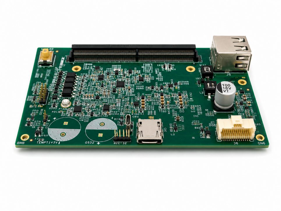
Custom carrier board design for System-on-Module (SOM) validation. The board shown is a SMARC-compliant reference implementation — one example within a broader capability to design carrier boards around other SOM standards and pinouts depending on the processor module and product requirements.

  • Full SMARC compliance
  • Adaptable to other SOM standards
  • Multi-vendor SOM evaluation
  • Signal-integrity-optimized layout
→
02
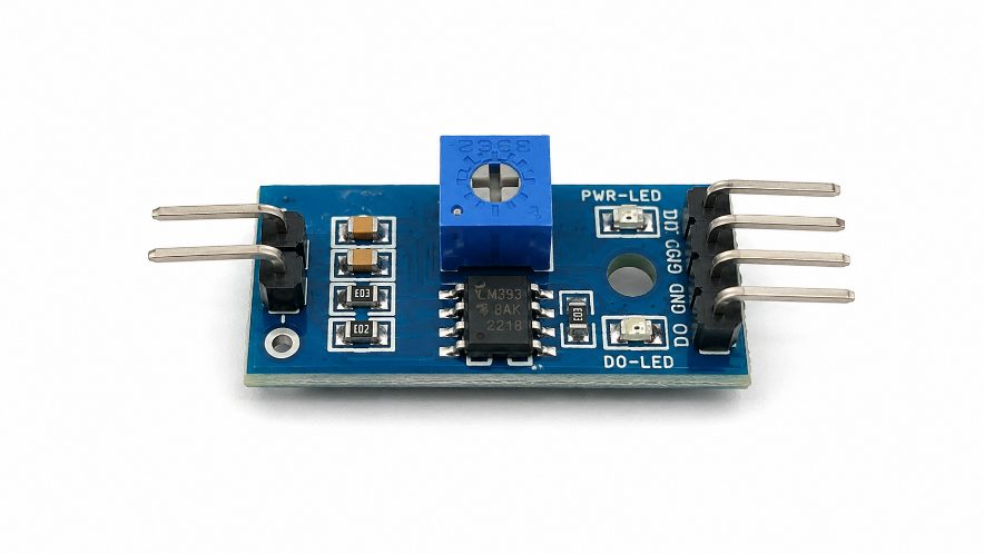
Opamp and BJT analog driver module
Rapid Prototype Validation · Opamp & BJT Reference Design

Analog Driver Modules

Compact, plug-and-play analog driver modules engineered to accelerate prototype validation. The module shown uses an opamp and BJT-based drive stage as a reference — the same design approach extends to other analog drive topologies selected to match project signal, load, and precision requirements.

  • Opamp / BJT reference design
  • Topology adaptable per project
  • Quick-connect bring-up headers
  • Amplification, conditioning & switching
→
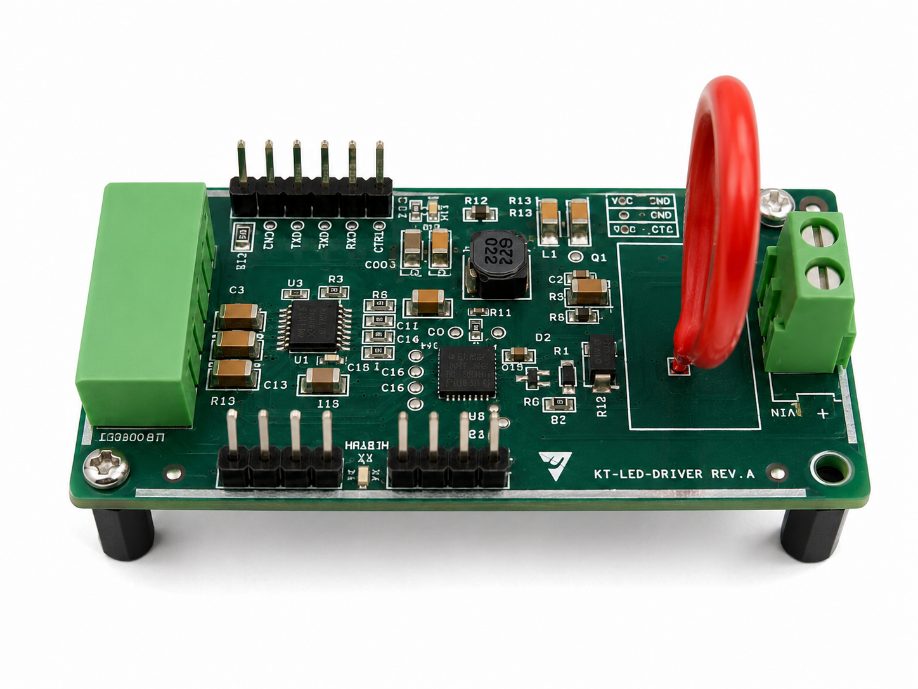
03
LED and display driver module
Plug-and-Play Lighting & Display · Configurable Drive Range

LED & Display Driver Modules

A family of LED driver modules engineered for plug-and-play validation of LEDs and lamp loads. The drive stage scales to other currents, voltages, and dimming or control protocols depending on the load, and the same platform extends to LCD display driving.

  • Plug-and-play LED / lamp driving
  • Scalable current & voltage range
  • LCD display driver support
→
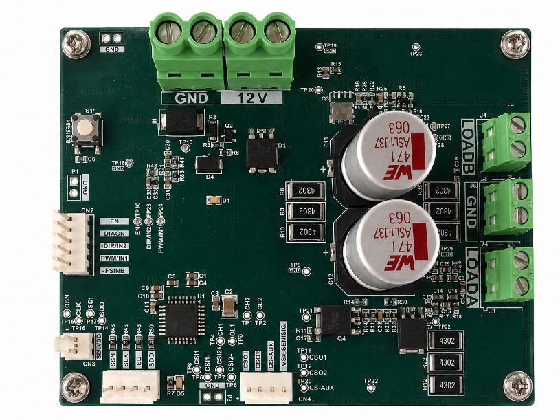
04
Motor driver module
Motion Control Validation · Multi-Topology Capability

Motor Driver Modules

Motor driver modules engineered for fast, dependable validation of motor control circuits during hardware bring-up. The design approach extends across DC, stepper, and BLDC topologies depending on the torque, speed, and control-loop requirements of the target application, with real-load testing built in.

  • Validated under real load
  • DC / stepper / BLDC capable
  • Plug-and-play integration
→
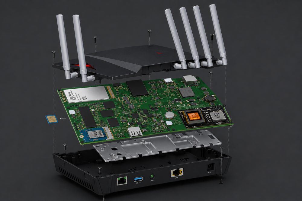
05
i.MX based router and gateway module
Embedded Networking · Multi-Platform Capability

Router & Gateway Design

Router and gateway modules engineered for configurable deployment as embedded network gateways. The platform shown is an NXP i.MX processor-based reference implementation — the design approach extends to other embedded processor platforms depending on throughput, connectivity, and cost requirements.

  • NXP i.MX reference platform
  • Adaptable processor selection
  • Configurable as network gateway
→
06
GPS and LTE connectivity module
IoT Connectivity Design · Multi-Module Capability

GPS & LTE Connectivity Modules

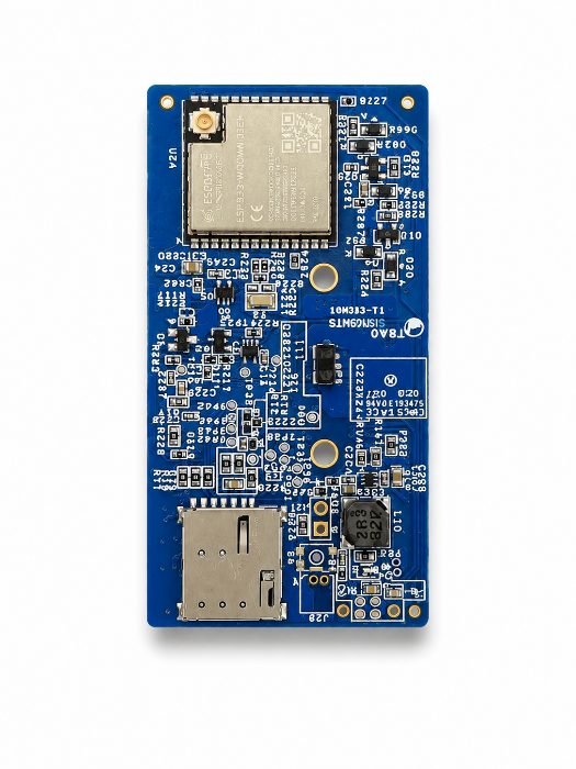
Cellular and positioning modules engineered for IoT connectivity validation, combining GPS positioning with LTE data connectivity on a single compact board. The design shown is built around the Quectel EG800 series — one reference implementation within a broader capability to design around other GNSS and LTE module families based on project band, carrier, and footprint requirements.

  • Quectel EG800-series reference
  • Adaptable to other GNSS/LTE modules
  • Integrated GPS + LTE
  • Rapid IoT device bring-up
→
05

Our Range of Services

S.01

Hardware Engineering

Production-ready electronics design from concept schematic through to manufacturable multilayer boards.

  • Schematic Design & Capture
  • Multilayer PCB Layout
  • High-Speed & Complex PCB
  • Low-Power Design
S.02

Embedded Systems & IoT

MCU, MPU, and SoC platform development across leading silicon, from wireless sensor nodes to cloud-ready gateways.

  • ESP32 / STM32 / NXP / TI
  • Board Bring-up & Debug
  • Wireless Sensor Nodes
  • Gateway & Telemetry Platforms
S.03

High-Speed Design

Signal-integrity-driven routing for demanding interfaces with controlled impedance and stack-up planning.

  • DDR3 / DDR4 Memory
  • USB 3.0 / Type-C PD
  • PCIe Gen 2/3
  • Gigabit Ethernet
S.04

Automotive Electronics

AEC-Q compliant hardware meeting automotive EMC and reliability standards for in-vehicle systems.

  • CAN / LIN Interfaces
  • AEC-Q Compliant Design
  • Automotive EMC Layout
  • Functional Safety Aware
S.05

Power & Battery Systems

Efficient, thermally sound power hardware engineered for safety and long battery life.

  • Battery Management (BMS)
  • Charging Circuits
  • Wireless & USB-PD Power
  • Power Management Design
S.06

Compliance, Test & Manufacturing

Pre-compliance design, systematic validation, and DFM discipline that carry your product cleanly to volume.

  • EMI / EMC Pre-Compliance
  • Prototype Bring-up & Test Jigs
  • DFM / DFA Review
  • Assembly & Production Liaison
06

Why Work With Us

One-Stop Studio

Concept, schematic, PCB, prototyping, and manufacturing readiness — every phase handled in-house, with no vendor handoffs or gaps.

Right the First Time

EMI/EMC-aware, DFM-oriented, standards-driven engineering that targets first-pass success over costly re-spins.

Proven Across Sectors

Deep experience across ESP32, STM32, NXP, and TI silicon, delivered across automotive, IoT, power, and industrial verticals.

Direct & Long-Term

Work directly with the engineer building your hardware, with ongoing support through the full product lifecycle.

07

Tools & Capabilities

The full stack, in-house. From first schematic to final assembly, every phase of hardware development is handled under one roof — no handoffs, no gaps, no finger-pointing between vendors.

EDA / Design

  • Altium Designer
  • Cadence Allegro
  • Cadence OrCAD
  • KiCAD

Processors Designed With

  • ESP32 Family
  • STM32 Family
  • NXP S32K / i.MX95
  • TI Jacinto J7 / AM2x

High-Speed Interfaces

  • DDR3 / DDR4 Memory
  • eMMC / NAND Flash
  • USB 3.0 / Type-C PD
  • PCIe Gen 2/3
  • Gigabit Ethernet

Additional Capabilities

  • Plastic Enclosure Support
  • Board Assembly Coord.
  • HW Validation & Testing
  • Complete Product Dev.
Open for new engagements

Let's Build Your
Next Product.

From concept to production — available for hardware design engagements, consulting, and full product development partnerships. Tell us what you're building.

Quick Contact